
Advanced Lithographic Micro Surfaces for Biodiagnostics
 P.G. Oppenheimer1 & J.J. Rickard1,2
1Advanced Nano-Materials, Structures & Applications (ANMSA), School of Chemical Engineering, University of Birmingham, UK
2Department of Physics, Cavendish Laboratories, University of Cambridge, Cambridge, UK
Medical diagnostics, environmental monitoring, homeland security and forensics increasingly demand specific and field-deployable analytical technologies for quick point-of-care diagnostics. Although technological advancements have made optical methods well-suited for miniaturization, a highly-sensitive detection technique for minute sample volumes is required. Raman spectroscopy is a well-known analytical tool, but has very weak signals and hence is unsuitable for trace level analysis. Enhancement via localized optical fields (surface plasmons resonances) on nanoscale metallic materials generates huge signals in surface-enhanced Raman scattering (SERS), enabling single molecule detection. This enhancement can be tuned by manipulation of the surface roughness and architecture at the sub-micron level. Nevertheless, the development and application of SERS has been inhibited by the irreproducibility and complexity of fabrication routes. The ability to generate straightforward, cost-effective, multiplex-able and addressable SERS substrates with high enhancements is of profound interest for SERS-based sensing devices. Herein, we briefly overview the work carried out in our group focussing on innovative routes to fabricate tuneable, low-cost, highly-sensitive surface-enhanced Raman scattering (SERS)-active miniaturised platforms to address the current challenges and pave the way for bio-diagnostic technologies which hold the potential for rapid, accurate and inexpensive disease diagnostics.
Raman scattering is dubbed after Sir Venkata Chandrasekhra Raman, who discovered and demonstrated the inelastic scattering of light from molecules in 1928. [1-2] Since then, Raman spectroscopy is increasingly implemented in the physical and chemical sciences. This vibrational spectroscopic technique is complementary to other IR techniques, and is based on the exchange of the energy of vibrational or rotational states of molecules with light, resulting in scattering of light with an altered wavelength. Rotational and vibrational Raman spectra (and their combination) can be recorded upon illuminating the sample with a monochromatic light. A red-shifted Stokes Raman spectrum is produced upon the inelastic scattering of the incident light with molecules in their rotational (or vibrational) ground state. Since at finite temperatures some molecules are also in excited states, a blue-shifted the anti-Stokes Raman spectrum forms when they interact with the incident light. The relative intensity of the Raman lines in both spectra can be used to determine the rotational or vibrational temperature.
Nearly five decades later, it was discovered that Raman scattering signals can be dramatically enhanced (by up to 106 fold) for molecules at structured noble metal based surfaces. [3] This SERS has enabled countless possibilities in sensitive analysis and diagnostics. The exact mechanism of the SERS effect is still debated in the literature. The current consensus regarding the underlying physics of this enhancement is based on the combination of an increased Raman cross-section of the molecules in contact with a metal submicrometer structure (chemical or electronic enhancement) and the electromagnetic field augmentation via localized optical fields of the metallic structures comprising the surface. These effects lead to several important properties of SERS: first, the enhancement scales as the fourth power of the local field near a metallic structure, and second, the enhancement is maximized when the incident light as well as the Raman scattered wave are in resonance with the surface plasmons of the metallic structure. SERS depends strongly on the surface on which the experiment is carried out.
The coupling of the surface field to excitations of adsorbed molecules causes an enhancement of Raman scattering by many orders of magnitude. [4-5] This leads to the requirement for the rational design and fabrication of surface structures to effectively enhance local electromagnetic fields for utilization of SERS in a range of applications, in particular in medical diagnostics. [6-7] Nanosphere self-assembly and standard lithographic techniques enable the manufacture of large area (irregular and ordered) SERS-active surfaces with intense electromagnetic ‘hot-spots’ which yield high SERS enhancement. [8] They can be however, inconsistent in terms of the measured signal and repeatability between different, although seemingly identical, substrates is difficult to achieve. [9-10] Electron-beam and photo-lithography are able to create sophisticated surface patterns for SERS, [11] but they typically require expensive and cumbersome, multi-step fabrication processes, which limit the scalability of the resulting structures. Alternative routes for multiscale structures include self-assembly or chemical processes [12] but, the precise control of features and prevention of defects remain a challenge, particularly in the sub-micrometer regime. The variable signal enhancement measured across single as well as (outwardly) identical SERS substrates further exacerbates the drawbacks of the current manufacturing processes. Moreover, while the advantages of periodically structured substrates for SERS have been demonstrated to enable improved enhancement, [13] reproducible and versatile platforms which allow the easy adjustment of structural parameters are still difficult to accomplish. These hindrances underline the constant need for versatile, cost-effective and straightforward methods to develop tunable three-dimensional structures that exhibit consistent and reliable signal enhancement across the surface. Thus, substrates with tuneable surface plasmon resonances matching the excitation lasers are needed to gain the highest enhancement for inexpensive, rapid SERS-based diagnostic applications. Over the past decade we have developed several SERS-active microsurfaces enabling high SERS enachment and rapid bio-analytes detection.
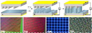 Figure 1. Schematics and optical images of pattern formation in thin polymer films in laterally heterogeneous electric fields. [22a]
One such approach is electrohydrodynamic lithography (EHL) which addresses certain setbacks described above while enabling the tuning of the LSPRs by generating a range of versatile micrometer sized structures with design geometries and periodicities. EHL harnesses instabilities in thin films induced by a lateral electric field variation, which causes the break-up of a thin polymer film and guides the material into design structures, allowing a one-step patterning of a broad range of architectures. Thus, EHL provides an important stepping stone towards generating reproducible, three-dimensional and long-range periodic SERS-active architectures. For high electric fields, the destabilizing electrostatic force overpowers the stabilizing effects of surface tension acting at the film-air interface. With time, this force imbalance causes an amplification of film undulations induced by the electric field (Fig.1), until they span the capacitor gap, thus leading to rearrangement to the energetically favoured configuration of the liquid. The polymer is destabilized first at the locations with the smallest inter-electrode spacing. The electrostatic pressure is much stronger for smaller electrode distances, pattern replication of topographically structured upper electrode proceeds at a shorter time scale than the regular EHD structure formation.
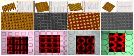 Figure 2. AFM and SEM images of high-fidelity EHL and Raman emission maps of the benzenethiol peak at 1070 cm-1 overlaid over an optical image of each patterned area generated patterns. [22b]
The pre-designed top electrode is highly reusable by employing self-assembled monolayer deposition, which is a standard way to reduce the surface energy while facilitating a non-destructive release of chemical and biological substances from metallic electrodes and can be hugely advantageous for calibration and long-term reusability. After coating with a plasmon-active metal such as gold, this provides versatile SERS-active substrates that overcome some of the typical drawbacks of other fabrication methods, which exhibit repeatable SERS enhancement from easily detectable structures under the optical microscope (Fig. 2).
The various EHD patterns show structure dependent SERS. For an optimized aspect ratio and geometry they give a 100-fold enhancement in SERS signals (Fig. 3). Considering that each of the individual structures gives such high enhancements the EHD patterned surfaces are a promising platform for multiplexed SERS detection. The demonstrated structures open up a range of further possible implementations including for instance advanced photo-catalysis and bio-analytics.
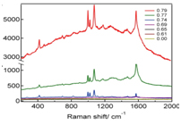 Figure 3. SERS spectra of benzene-thiol recorded from substrates with EHL pillars. [23]
Depending on the structure and inter-structure spacing, certain periodic arrays exhibited SERS enhancement either at their perimeter or in the area between the structures. Further, polarization-dependent SERS is detected at the interstitial locations of the periodic structures (Fig. 4). The EHL technique offers a great variability of structural features by the independent control of several parameters in a robust fashion, generating high-fidelity uniform patterns across large substrate areas. It thus provides a complementary platform for the reliable manufacture of substrates with consistent SERS enhancements. The tuning of plasmon resonances is further accomplished by controlling the dimensions, geometry and aspect ratio of the EHL-generated pillar arrays. This tuneability allows the design of SERS substrates that generate strong localized electromagnetic fields at optical wavelengths that are required for the optimum SERS excitation by different laser sources. Overall enhancement factors up to 107 were reproducibly obtained. The polarization-dependent surface-enhanced Raman scattering reveals the highest intensity at the interstitial locations of the periodic structures. The ability to carefully design highly reproducible periodic arrays enables the control of localized plasmonic fields for a variety of lab-on-chip sensing devices. The polarisation effect presents an additional degree of freedom for the use of EHL-generated platforms for switchable nanophotonic devices and multiplexed SERS detection at the local microstructure-level.
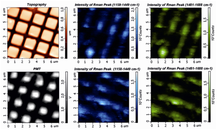 Figure 4. AFM tapping mode topography and confocal image of the backscattered Rayleigh signal at 633 nm. Raman scattering obtained simultaneously with NT-MDT VIT_P cantilevers which with a laser spot focussed on the tip apex, confirming the SERS activity of the EHL generated structure. Raman mapping with vertically and horizontally polarized excitation. [22]
Carbon nanotubes (CNTs) have been, concurrently, a topic of extensive research and applications, in particular because of their extraordinary electrical, thermal, and mechanical properties. [14-17]
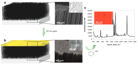 Figure 5. Fabrication of well-ordered large-area gold coated VACNT SERS-active platforms. [24]
However, the application of CNTs for plasmonics including SERS has been only recently beginning to gain interest. [18-20] These studies use nanoparticle-functionalized CNTs for SERS and consequently their reproducibility and stability, and hence their practical applications remain debatable. Recently, Milne and coworkers reported the modeling and use of large diameter multiwalled carbon nanotubes (MWNTs) coated with silver as antennae for enhancing Raman signals, [21] although for practical SERS applications, gold coating, being more inert and stable, is more suitable compared to silver. However, none of the studies have paid attention to the structural parameters for optimization of CNT-based substrates for SERS. Control and understanding of the role of structural parameters for the generation of “hot-spots” is necessary to take full advantage of the synergistic functions of CNT-based SERS architectures. Furthermore, the utilization of VACNT forests for SERS remains rather unexplored. VACNTs can provide low-cost, simple, large-active-area patternable substrates which, through appropriate functionalization, will be able to provide advanced SERS platforms.
We have generated gold-coated VACNT forests as SERS substrates which have been shown to deliver high reproducible enhancements of the order of 107 and over large areas of 5 × 5 mm2 and above (Fig. 5). The enhancement properties of the VACNTs- Au SERS substrates have found to be highly dependent on the structural parameters of the CNTs, such as diameter and distance (Fig. 6). These factors are configured using straightforward process control (i.e., control of the catalyst or growth conditions). VACNTs with an increased relative density and smaller diameters yield higher Raman signal enhancements.
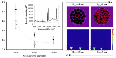 Figure 6. Relative enhancement dependence on nanotube diameters with the corresponding SERS spectra at constant forest density. [24]
Therefore, by altering the above key parameters VACNTs gold-coated substrates can be tuned and tailored to provide advanced applications. Furthermore, the dependence of SERS enhancements is verified and found to be consistent with EM simulations. Finally, we have shown that patterned arrays of CNTs can be fabricated to give multiplexed SERS detection (Fig. 7). Such unique combination of materials and nanospectroscopic platforms is promising for a variety of applications in chemical and biological sensing.
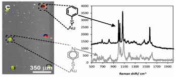 Figure 7. Lithographically defined VACNT-Au platforms for multiplex SERS detection. [24]
In this article we have over-viewed a small portion of the work that we have carried out on SERS-active platforms in the past few years at both the University of Cambridge and the University of Birmingham. We continue working on developing intelligently engineered, carefully designed and optimised SERS-based devices which may ultimately enable the next-generation sensing technologies fulfilling multitude criteria.
References
[1]. CVKKS. Raman, Nature, 121:501, 1928.
[2]. B Schrader and D Bougeard, Wiley-VCH, Weinheim, 1995.
[3]. M. Fleischmann, P.J. Hendra, and A.J. McQuillan, Chemical Physics Letters, 26(2):163, 1974.
[4]. Barnes, W. L.; Dereux, A.; Ebbesen, T. W, Nature 2003, 424, 824.
[5]. Ozbay, E. Science 2006, 311, 189.
[6]. Tripp, R. A.; Dluhy, R. A.; Zhao, Y. Nano Today 2008, 3, 31.
[7]. Patel, I. S.; Premasiri, W. R.; Moir, D. T.; Ziegler, L. D. 2008, 39, 1660.
[8]. Chou, S. Y.; Krauss, P. R.; Renstrom, P. J. Science 1996, 272, 85.
[9]. Netti, C.; Lincoln, J.; Flinn, G. Raman Technology for Today’s Spectroscopists 2005, 3.
[10]. Etchegoin, P. G.; Le Ru, E. C. Phys. Chem. Chem. Phys. 2008, 10, 6079.
[11]. Kahl, M.; Voges, E.; Kostrewa, S.; Viets, C.; Hill, W. Sensors and Actuators B: Chemical 1998, 51, 285.
[12]. Yan, B.; Thubagere, A.; Premasiri, W. R.; Ziegler, L. D.; Dal Negro, L.; Reinhard, B. M. ACS Nano 2009, 3, 1190. [13]. Kahl, M.; Voges, E.; Kostrewa, S.; Viets, C.; Hill, W. Sensors and Actuators B: Chemical 1998, 51, 285.
[14]. Sun, Y.-P.; Fu, K.; Lin, Y.; Huang, W. Acc. Chem. Res. 2002, 35, 1096.
[15]. Dresselhaus, M. S.; Dresselhaus, G.; Jorio, A., Ann. Rev. Mater. Res. 2004, 34, 247.
[16]. Qu, L.; Vaia, R. A.; Dai, L. Multilevel, ACS Nano 2011, 5, 994.
[17]. Kinoshita, H.; Kume, I.; Tagawa, M.; Ohmae, N.; Turq, V.; Martin, J. M. International Tribology
Conference, Kobe 2008.
[18]. Beqa, L.; Singh, A. K.; Fan, Z.; Senapati, D.; Ray, P. C. Chem. Phys. Lett. 2011, 512, 237.
[19]. Wang, X.; Wang, C.; Cheng, L.; Lee, S.-T.; Liu, Z. J. Am. Chem. Soc. 2012, 134, 7414.
[20]. Chu, H.; Wang, J.; Ding, L.; Yuan, D.; Zhang, Y.; Liu, J.; Li, Y. J. Am. Chem. Soc. 2009, 131, 14310
[21]. Dawson, P.; Duenas, J. A.; Boyle, M. G.; Doherty, M. D.; Bell, S. E. J.; Kern, A. M.; Martin, O. J. F.; Teh, A. S.; Teo, K. B. K.; Milne, W. I.. Nano Lett. 2011, 11, 365.
[22a]. Goldberg Oppenheimer, P. Steiner, U. Small, 2010, 1248.
[22b]. Mahajan, S., Hutter, T., Steiner, U., Goldberg Oppenheimer, P. J. Phys. Chem. Lett., 2013, 4 (23),
4153.
[23]. Goldberg-Oppenheimer, P., Mahajan, S., Steiner, U., Adv. Mater. 2012, 24, OP175.
[24]. Goldberg-Oppenheimer, P., Hutter, T., Chen, B., Robertson, J., Hofmann, S., Mahajan, S. J. Phys.
Chem. Lett. 2012, 3, 3486.

Meet Our Editors

Advert Logos