
High-Efficiency High-Temperature Cells for Solar Concentrating Systems
The ProME3ThE2US2 project – Production Method of Electrical Energy by Enhanced Thermal Electron Emission by the Use of Superior Semiconductors (www.prometheus-energy.eu) – aims at developing, validating and implementing novel solid-state structures able to convert directly concentrated solar radiation into electric energy, at a very high efficiency. The project objective is the development of efficient solar concentrating cells, based on engineered semiconductors, able to overcome the limitations of multiple-junction cellswhen operating at high-temperature. ProME3ThE2US2 is a European collaborative project within the Energy FP7 framework of Future Emerging Technologies (FET). Coherently with the FET strategy based on high risk research, the project aims at incubating and developing a breakthrough concept for concentrated solar conversion, with a very high technological impact.
The core conversion mechanism is obtained by an enhanced electron emission. The cathode, made of advanced semiconductor structures, operates as a photo-thermionic cathode (PETE – Photon-Enhanced Thermionic Emission device, firstly demonstrated by Stanford University [J.W.Schwede et al., Photon-enhanced thermionic emission for solar concentrator systems, Nature Materials 9 (2010) 762]), taking advantage of the high temperature it can achieve from the absorption of the IR part of solar radiation (not able by itself to induce charge carrier production), and from thermalization of the excess energy of charge carriers generated by interaction with solar light.The efficiency of this solid-state technology, analyzed by advanced simulation methods and performed by the groups of the Tel Aviv University involved in the project, can be as high as 52% under concentrating systems able to provide a solar radiation flux of 1000 suns. Combined to a secondary thermal cycle, the system efficiency limit increases up to the outstanding value of about 70% [G. Segev et al., Limit of efficiency for photon-enhanced thermionic emission vs. photovoltaic and thermal conversion, Solar Energy Materials & Solar Cells 140 (2015) 464]. The system may be also cogenerative, thus supplying additional exhaust thermal energy as an output for more completely supplying the needs of future end-users for domestic and rural applications.
A general sketch of the system is depicted in Fig. 1. The solid-state converter operates under vacuum conditions to allow emitted electrons travel from the cathode to the anode. Although vacuum conditions could be considered a technological complication, on the other hand they allow a substantial reduction of heat losses. The concentrated solar radiation impinges on the converter through a transparent window. The engineered cathode is mechanically supported by a transparent substrate in order to be optically inherent to the radiation. An optional IR absorber can be deposited on one surface of the transparent substrate, aimed at transforming into heat the energy of IR photons, not able to induce charge photogeneration. The IR absorber has to be transparent to the remaining part of the solar spectrum in order not to interfere with the operability of the active absorber. The absorber is generally a thin-film (from tenths to few micrometers) deposited on the second surface of the transparent substrate, and has the function to capture the most part of the solar spectrum, converting it into electric charges. By designing a proper band structure, electrons can be injected into the last thin coating, developed directly onto the absorber (thickness less than tens of nanometers), characterized by a low work function to allow an efficient electron escape towards vacuum. Emitted electrons have to travel in vacuum for a short distance (few micrometers) aimed at avoiding space charge effects: to satisfy this condition, a specific technology for fabricatingthermally and electrically insulating micro-machined spacers is under development. Emitted electrons have to be finally collected by an anode consisting of a substrate (usually metal, to decrease the converter series resistance) coated by a film able to guarantee a lower work function than the cathode one (this is a condition to achieve a steady-state current with no bottlenecks). The exhaust heat on the anode, produced in most part from the thermal irradiance from the cathode operating at higher temperatures, can feed a secondary thermal cycle of conversion based (but not limited to) on the use of thermomechanical engines. In other words, the PETE device acts as a topping cycle for additional conversion stages, with a total efficiency resulting in a linear combination of the efficiencies of each stage. Several technological and scientific concepts are combined within the project activities.
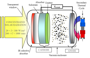 Fig. 1. Operating sketch of the high-temperature solar cell.
Band gap & Defect Engineering Strategies for the Cathode
Two alternative cathode technologies proposed by ProME3ThE2US2 include extremely ambitious and innovative concepts, guided by the predicting analysis provided by advanced simulation models.The first is founded on a bandgap engineering strategy of the active semiconducting layers by developing semiconductors with a bandgap matched to the solar spectrum (the most proper value is 1.8 eV). This aim can be pursued with III-V semiconductors, and specificallyby tailoring the crystal composition and physical properties of GaInP and InGaN structures developed by the Fraunhofer Institute for Solar Energy and by the multinational Abengoa Research, respectively. The aim is obtaining high levels of crystallinity to guarantee the photo-generated electrons the longest possible travel within the absorber material towards the emitting layer. For phosphide-based cathode, a novel technology is being exploited: wafer bonding enables the layer structures transfer from the GaAs growth substrate to a transparent sapphire wafer. On the other hand, nitride-based structures are directly fabricated on a transparent sapphire wafer. But III-V semiconductors do not natively show low work-functions, that represents the primary property for the efficiency of a cathode: they need an additional very thin coating of a material characterized by a low work-function to allow electron emission. BaO and LiO are alkali-based materials that guarantee higher stability than pure alkaline metals are under development within the project by Solaris Photonics Ltd.
The second cathode technology is based on a defect engineering strategy performed on advanced IV semiconductors, among which our attention is mainly focused on CVD diamond. Diamond has an exclusive characteristic: the work function can be significantly reduced by hydrogenating its surfacein order to allowelectrons an easy escape towards the vacuum. Hydrogen atoms at the diamond surface induce a strong negative electron affinity, making it the best candidate for an efficient thermionic cathode. Hydrogen on carbon is very stable up totemperature of 780 °C giving a high operational robustness to a diamond cathode. On the other hand, diamond has a wide bandgap of 5.47 eV, corresponding to a high transparency to the solar spectrum, so it does not interact with the solar radiation. This issue is tackled by introducing localized defect states in the diamond bandgap, allowing itabsorb solar photons and exploit them into a useful photo-induced current. Two parallel, opposite sub-strategies are under development in the project: i) nano- and/or micro-crystalline diamond thin-films with a controlled defect density, developed by Technion Institute of Technology, and containing graphitic grain boundaries able to absorb IR and acting as distributed electric contacts for a reduction of cathode series resistance [S. Elfimchevet al., The impact of surface hydrogenation on the thermionic electron emission from polycrystalline diamond films, Phys. Status Solidi A 211 (2014) 2238–2243]; ii)”black” diamond photo-thermionic cathodes, characterized by a surface texturing with a sub-micrometer periodicity comparable to the solar radiation wavelength [P. Calvani et al., Optical Properties of Femtosecond Laser Treated Diamond, Applied Physics A, 117 (2014) 25-29]. Surface texturing of CVD diamond plates by ultrashort laser pulses was demonstrated by the Consiglio Nazionaledelle Ricerche to significantly increase their optical absorption (Fig. 2 shows the resulting “black” diamonds and Fig. 3 the nanostructure inducing the specific optical property). Moreover, the treatment, if performed to form periodic nanostructures results in a considerably enhanced responsivity, even higher than expected from optical absorbance, indicative of the formation of defined electronically active bands within the diamond bandgap. In order to reduce the cathode series resistance for thermal electrons, a specific 3D graphitization technology based on fs-laser treatment was performed to form high electric conductivity graphitic columns. Finally, ion implantation of boron was demonstrated to have a positive effect both on the optical absorption and on the responsivity. These three technologies are going to be combined together for developing the single-crystal diamond cathode.
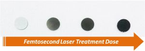 Fig. 2. Diamond plates become black-diamond.
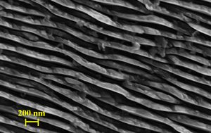 Fig. 3. Periodic nanostructures inducing the diamond to be black.
Anode technology
The work function of the anode has to be lower than the cathode one for maximizing the electron flow and, consequently, the device conversion efficiency. In all the thermionic energy converters, a continuous run occurs between the development of low work-function cathodes, able to dramatically increase emitted currents, and a consequent development of even lower work-function anodes. Pure alkali metals (cesium, barium) have been used in the past, but they revealed an operative instability at high temperature. BaO and LiO thin layers, more stable than the pure metal elements, are under development on engineered refractory metals substrates with the aim to reduce the device series resistance, with additional desirable properties of reflecting as much as possible the black body radiation emitted by the cathode, and getter capability, to contribute maintaining high vacuum levels for future encapsulated device versions.
Inter-electrode spacing
The development of a spacer able to maintain a vacuum gap between the electrodes of few micrometers is a primary condition for the efficiency of every thermionic energy converter. The optimal gap value mainly depends on the cathode operating temperature: gaps larger than few micrometers induce severe conditions of space charge, responsible for a strong reduction of the emission current. Conversely, gaps narrower than the optimal one are not desirable since the anode receives the effect of the near-field radiative energy transfer from the hot cathode, resulting in an excessive anode heating. The proposed technological solution is based on the development of micro-machined thermally and electrical spacers, fabricated directly on the anode surface by the Italian SME Ionvac Process Srl. Micromachining represents an advanced technology to guarantee a robust gap definition and to minimize the cathode/spacer/anode contact area, so to consequently reduce the thermal flow between the electrodes. The materials under development are zirconium and aluminum oxides fabricated by employing advanced microtechnologies. Finally, the secondary thermal cycle, which, being a consolidated technology, is analyzed only through comparative simulations performed by the British SME Exergy Ltd on consolidated solutions present in the market.
The project activity is atits mid-term. Four different semiconductor structures are under a dynamic development. ProME3ThE2US2 is pushing each semiconductor technology to the limits by also applying original concepts for achieving the result of making efficient high-temperature solar cells come true.
Contact details: Project coordinator Daniele M. Trucchi, PhD
CNR – ISM (Institute of Structure of Matter)
Research Area Roma 1 – Via Salaria km 29.300
00015 – Monterotondo Scalo (Rm) – Italy
Email: daniele.trucchi@ism.cnr.it
Tel. +39 0690672-558 (-252, -233, -243); Fax +39 0690672-238
Project Consortium
| Partner | Nation | Type | Team Leader |
| ConsiglioNazionaledelleRicerche | Italy | Research Centre | Dr. Daniele M. Trucchi |
| Tel Aviv University | Israel | University | Prof. Abraham Kribus |
| Technion Institute of Technology | Israel | University | Prof. Alon Hoffman |
| Fraunhofer Institute | Germany | Research Centre | Dr. Frank Dimroth |
| Ionvac Process Srl | Italy | Hi-Tech SME | Mr. Aniello Vitulano |
| Exergy Ltd | U.K. | Hi-Tech SME | Dr. Fernando Centeno |
| Solaris Photonics Ltd | U.K. | Hi-Tech SME | Dr. Arnaldo Galbiati |
| Abengoa Research SL | Spain | Industry | Dr. Veronica Carcelen |
 Fig. 4. The consortium members and the Project Officer during a project meeting in Freiburg (Germany) at the Fraunhofer Institute for Solar Energy.

Meet Our Editors

Advert Logos