
Carbon Based Electronics
W. I. Milne & M. T. Cole
Electrical Engineering Division, Department of Engineering, Cambridge University, UK
Over the past few decades, there have been many major advances in the field of electronics due, in the most part, to the continued miniaturisation of Si-based electronic devices. Regardless of the consistent push for ever small consumer electronics, we are, however; swiftly reaching the technological “wall” and will soon encounter both technical and scientific limits. There have been various attempts to address this problem by movement away from conventional device structures. Another approach has been to investigate the use of alternative material systems, some of which could be used on flexible substrates. Here we will briefly describe some of the work carried out over the past couple of decades in our Department on the realisation of Carbon Based Electronics as one possible solution to this ubiquitous problem.
In the late 1980’s, early 1990’s, there was an increasing interest in the use of carbon based materials for use as an active electronic material in devices, and also in a plethora of passive applications. In our laboratory, as we had been working on amorphous silicon (specifically hydrogenated amorphous silicon (a-Si:H) for several years), the move to investigate amorphous carbon, and the various carbon allotropes, was a very obvious one. Diamond-like-carbon (DLC) is a metastable form of amorphous carbon (a-C) containing a significant proportion of sp3 bonds. A ternary phase diagram of bonding in a-C hydrogen alloys1 is shown in Figure 1.
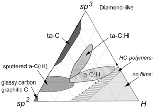 Figure 1. Ternary phase diagram of amorphous carbon (a-C). Adapted from 1
Our interest focussed on two variants of DLC, the first material – hydrogenated amorphous carbon (a-C:H) which could be produced using plasma enhanced chemical vapour deposition (PECVD) in a somewhat similar manner to a-Si:H production and tetrahedrally bonded amorphous carbon (ta-C) which we produced using a Filtered Cathodic Arc process.
The high sp3 bond concentration of DLC results in a very mechanically hard material that is chemically and electrochemically inert and has a wide band gap, similar to diamond itself. This led it to being used in a plethora of applications including anti fuses,1 low dielectric constant films,1 field emitters,2 and as the active layer in field effect transistors (FETs).3 However, the performance of DLC in FETs was poor. DLC typically possesses a large density of states in the bandgap.3 It transpired, that the mechanical properties of the DLC made it much more useful in mechanical applications, as for example, in protective coatings1 and in micro-electromechanical devices where it could be utilised in the manufacture of novel normally closed microgrippers, as shown in Figure 2.4
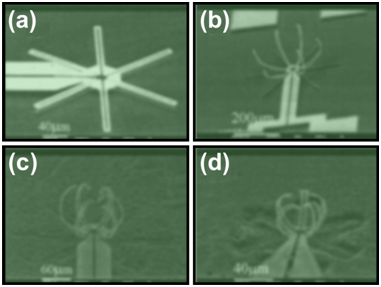 Figure 2. (a) SEM images of a Ni microgripper frame (without a DLC layer) with a finger length of 100 µm; (b)–(d) SEM images of devices with various DLC/Ni thickness ratios and finger length. (d) Shows a fully closed microcage with a diameter of around 40 μm.4
The films are also remarkably smooth and can be deposited at room temperature and have excellent coverage on a variety of substrates. This has led to their use in perhaps its most major application to date – the protective coating on digital recording heads and disks1. Thus, although there was some success in the optimisation of amorphous carbon thin films, its use in active electronic devices largely failed to materialise and it is its mechanical properties which have proven to be of much greater industrial interest.
Our own interest in carbon based materials, however; did not end there. Just as our work on the electronic applications of DLC was coming to a conclusion, we began work on carbon nanotubes (CNTs). CNTs are allotropes of graphitic carbon with a cylindrical structure. Most single wall nanotubes (SWCNTs) have diameters of ~ 1 nm and are either semiconducting or metallic-like. Multiwall CNTs (MWCNTs) consisting of several concentric nanotubes (somewhat like a Russian–Doll structure), which can be ~ 20 – 100 nm diameter and are always metallic-like in nature. There are a plethora of potential electronic applications for CNTs but many such applications depend on techniques of selectively producing (or post growth separation of) either semiconductor or metallic CNTs. It is possible using a novel Chemical Vapour Deposition (CVD) recipe using methanol and ethanol mixtures to grow > 95% semiconductor tubes,5 but there is still no way to grow 100% semiconducting tubes. Alongside many other groups, we investigated the use of CNTs (both individual and networks) to produce transistor structures (Figure 3).6 Since then, various groups have optimised the process and most recently the group in Stanford7 have announced the first CNT based “computer”, with IBM identifying CNTs as excellent semiconductors for the replacement of Si8 going forward.
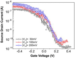 Figure 3. Gate transfer characteristics of a top-gate CNT FET (Vds=50, 100, 200 mV).6
However, our own major interests lies in the use of CNTs for field electron emission applications and their use in replacement of copper for interconnects and vias in very large scale integration (VLSI) circuits because of their high thermal stability, thermal conductivity and electrical conductivity. In this instance, although individual CNTs can carry current densities of order 4×10⁹ A/cm2, the main obstacle to their use is in the ability to produce sufficiently high areal packing densities to meet the actual currents required. By careful control of the growth process,9 Robertson and co-workers have successfully produced inter-connects based on metallic-SWCNTs forests by controlling the catalyst thickness to increase the CNT overall areal density from ~1012 cm-2 to ~1.5 x1013 cm-2. Of course, there is still some way to go before such structures can be made within vias on actual integrated circuits.
Ever since the invention of the micro-tip field emitter source by Spindt and co-workers,10 there have been numerous attempts to achieve more efficient and stable electron sources. Indeed, we spent some time investigating the use of DLC as field emitters in the 1990’s11 but have, more recently focussed on CNTs because of their high aspect ratio and near-ideal whisker-like shape. CNTs have other properties which lend themselves to the fabrication of efficient field emission sources – they have an exceedingly high room temperature conductivity and, as they are covalently bonded, they do not suffer from electro-magnetism. CNTs have already been demonstrated in a wide variety of application and in our particular case we have utilised them in field emission displays2 in collaboration with Samsung and as sources for electron microscopes12 (Figure 4).
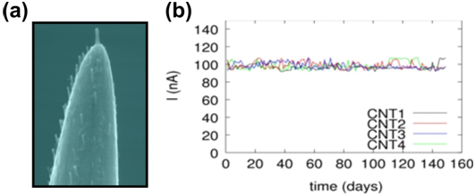 Figure 4. (a) CNT grown on top of W tip (b) Life-time measurements of 4 individual CNT electron sources mounted on W tips ( courtesy of N.De Jonge).12
We have also investigated the use of CNT-based electron sources in parallel electron beam lithography,13 and as sources in high frequency generators/amplifiers, both in collaboration with Thales.14 Figure 5 shows schematically a single element of a writing head for a parallel electron beam lithography system and an example of a microfabricated CNT emitter needed for each source is shown in Figure 5(b) where a 2 μm gate aperture is used and a 100 nm diameter MWCNT is produced using a self–aligned technology. For a 100×100 array the emitted current which reaches the anode, was 10 mA, equivalent to 1 nA per emitter.
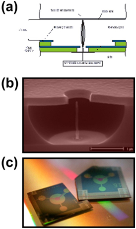 Figure 5. (a) Schematic of parallel electron beam lithography source (b) integrated CNT in gate (c) 10×10 mm micro-cathodes.12
In 14 we described the construction of a microwave diode where the CNT field emission source was directly driven at gigahertz (GHz) frequencies. Arrays of vertically aligned MWCNTs, as shown in Figure 6(a), were integrated onto a coaxial post in a resonant cavity. In the device simulation shown in Figure 6(c), radiofrequency electromagnetic radiation at the input induces a high, oscillating electric field at the end of the coaxial post; this electric field is further amplified by the MWCNT array. Successful operation at 1.5 GHz was obtained at a current density of 12 A/cm2.
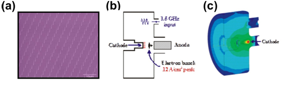 Figure 6. (a) A scanning electron micrograph of a typical MWCNT array grown by PECVD. (b) Schematic of a microwave cavity design and corresponding (c) simulation. Adapted from 14.
Most recently we have been investigating the use of CNTs in X-ray sources and have begun collaboration with Cambridge X-ray Systems; our aim, to produce stable, long lifetime sources. In order to do this we have produced individually ballasted CNT structures. One such silicon-on-insulator (SOI) ballasted emitter array is shown in Figure 7(a). Here each MWCNT emitter is connected in series to a single FET formed from the upper most Si layer and back-gated by the Si.
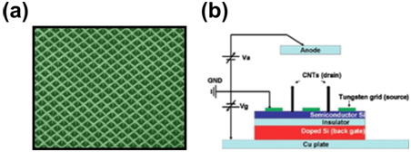 Figure 7. (a) A scanning electron micrograph of a fabricated ballasted array of MWCNTs, and (b) schematic of measurement process.15
The potential drop across the FET channel tends to limit the rise in emission current by reducing the tip-to anode potential difference. The FET is formed from an undoped Si channel on a 200 nm thick thermally oxidized SiO2 gate dielectric with asymmetric source-drain contacts. The source is formed from a square W mesh contacting the polycrystalline Si. W is an abundant source of electrons when connected to the negatively biased power supply. The drain contact is formed at the MWCNT/catalyst junction at the base of the MWCNT. The drain receives electrons in response to transport through the channel, but cannot source them. As the current increases, the potential at the drain becomes increasingly positive. Thus, the gate-drain potential difference reduces which saturates the emitted current. By electronically controlling the source-drain potential we have demonstrated the ability to controllable limit the emission current density by more than one order of magnitude. The detailed fabrication procedure is found in 15. CNTs, utilising mis-orientated mats, have already been used in commercial products by XinRay Systems in the USA where their CNT x-ray source array based stationary computed tomography provides high speed, high resolution, and a small footprint.16
We continue to look at further commercial applications for CNTs but our latest interest in carbon based electronics, like many other groups, is in the production and application of graphene. Our first effort was in the area of field emission where we utilised graphene as actual field emitter.17 However our major innovation in this area was to use graphene, not as an emitter, but rather in a novel gate structure. Here we used CVD synthesised graphene films as the gate electrode in a triode field emission source structure and compared it to a standard mesh gate.18
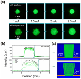 Figure 8. A graphene based gate electrode in field emission triodes. (a) Integrated intensity maps showing the electron beam divergence with graphene (top) and without (bottom). (b) Extracted beam diameters, and (c) simulated beam divergence for gates with (top) and without (bottom) graphene.18
The highly electron transparent gate electrodes were fabricated from chemical vapour deposited bilayer graphene transferred to Mo grids with experimental and simulated data, showing that emitted electrons (from screen printed MWCNT films) efficiently traverse the graphene membranes with transparencies in excess of 50–68%. The graphene hybrid gates are shown to reduce the gate driving voltage by 1.1 kV, whilst increasing the electron transmission efficiency of the gate electrode significantly. As shown in Figure 8(a), integrated intensity maps show that the electron beam angular dispersion is dramatically improved coupled with a 63% reduction in beam diameter.18
In this paper we have reviewed a small selection of the work that we have carried out on Carbon Based Electronics in the Electrical Division of the Engineering Department, Cambridge University, over the past twenty years. We continue to work on CNTs and graphene in order to continue to develop ever more functionally enhanced electron sources and novel electronic devices that may ultimately realise real-world devices on an all-carbon platform.
Acknowledgements
We would like to acknowledge all the help, collaboration and support from our colleagues; Gehan Amaratunga, John Robertson, Ken Teo and Manish Chhowalla, alongside all present and past post docs, PhD students and our co-workers worldwide, who continue to make, our work possible.
References
- Robertson, J. Diamond-Like Amorphous Carbon. Materials Science and Engineering: R: Reports 2002, 37, 129-281.
- Milne, W. I.; Teo, K. B. K.; Amaratunga, G. A. J.; Legagneux, P.; Gangloff, L.; Schnell, J. P.; Semet, V.; Binh, V. T.; Groening, O. Carbon Nanotubes as Field Emission Sources. J. Mater. Chem. 2004, 14, 933-943.
- Clough, F. J.; Milne, W. I.; Kleinsorge, B.; Robertson, J.; Amaratunga, G. A. J.; Roy, B. N., Tetrahedrally Bonded Amorphous Carbon (Ta-C) Thin Film Transistors. In Electron. Lett., Institution of Engineering and Technology: 1996; Vol. 32, pp 498-499.
- Luo, J. K.; He, J. H.; Fu, Y. Q.; Flewitt, A. J.; Spearing, S. M.; Fleck, N. A.; Milne, W. I. Fabrication and Characterization of Diamond-Like Carbon/Ni Bimorph Normally Closed Microcages. Journal of Micromechanics and Microengineering 2005, 15, 1406.
- Yang, F.; Wang, X.; Zhang, D.; Yang, J.; LuoDa; Xu, Z.; Wei, J.; Wang, J.-Q.; Xu, Z.; Peng, F., et al. Chirality-Specific Growth of Single-Walled Carbon Nanotubes on Solid Alloy Catalysts. Nature 2014, 510, 522-524.
- Yang, M. H.; Teo, K. B. K.; Gangloff, L.; Milne, W. I.; Hasko, D. G.; Robert, Y.; Legagneux, P. Advantages of Top-Gate, High-K Dielectric Carbon Nanotube Field-Effect Transistors. Appl. Phys. Lett. 2006, 88, 113507.
- Shulaker, M. M.; Hills, G.; Patil, N.; Wei, H.; Chen, H.-Y.; Wong, H. S. P.; Mitra, S. Carbon Nanotube Computer. Nature 2013, 501, 526-530.
- Park, H.; Afzali, A.; Han, S.-J.; Tulevski, G. S.; Franklin, A. D.; Tersoff, J.; Hannon, J. B.; Haensch, W. High-Density Integration of Carbon Nanotubes Via Chemical Self-Assembly. Nat Nano 2012, 7, 787-791.
- Zhong, G.; Warner, J. H.; Fouquet, M.; Robertson, A. W.; Chen, B.; Robertson, J. Growth of Ultrahigh Density Single-Walled Carbon Nanotube Forests by Improved Catalyst Design. ACS Nano 2012, 6, 2893-2903.
- Spindt, C. A. A Thin-Film Field-Emission Cathode. J. Appl. Phys. 1968, 39, 3504-3505.
- Satyanarayana, B. S.; Hart, A.; Milne, W. I.; Robertson, J. Field Emission from Tetrahedral Amorphous Carbon. Appl. Phys. Lett. 1997, 71, 1430-1432.
- Mann, M.; Teo, K.; Milne, W.; Tessner, T. Direct Growth of Multi-Walled Carbon Nanotubes on Sharp Tips for Electron Microscopy. Nano 2006, 1, 35-39.
- Teo, K. B. K.; Chhowalla, M.; Amaratunga, G. A. J.; Milne, W. I.; Legagneux, P.; Pirio, G.; Gangloff, L.; Pribat, D.; Semet, V.; Binh, V. T., et al. Fabrication and Electrical Characteristics of Carbon Nanotube-Based Microcathodes for Use in a Parallel Electron-Beam Lithography System. Journal of Vacuum Science and Technology B 2003, 21, 693-697.
- Teo, K. B. K.; Minoux, E.; Hudanski, L.; Peauger, F.; Schnell, J. P.; Gangloff, L.; Legagneux, P.; Dieumegard, D.; Amaratunga, G. A. J.; Milne, W. I. Microwave Devices – Carbon Nanotubes as Cold Cathodes. Nature 2005, 437, 968-968.
- Li, C.; Zhang, Y.; Cole, M. T.; Shivareddy, S. G.; Barnard, J. S.; Lei, W.; Wang, B.; Pribat, D.; Amaratunga, G. A. J.; Milne, W. I. Hot Electron Field Emission Via Individually Transistor-Ballasted Carbon Nanotube Arrays. ACS Nano 2012, 6, 3236-3242.
- Liu, Z.; Yang, G.; Lee, Y. Z.; Bordelon, D.; Lu, J.; Zhou, O. Carbon Nanotube Based Microfocus Field Emission X-Ray Source for Microcomputed Tomography. Appl. Phys. Lett. 2006, 89, 1-3.
- Hallam, T.; Cole, M. T.; Milne, W. I.; Duesberg, G. S. Field Emission Characteristics of Contact Printed Graphene Fins. Small 2014, 10, 95-99.
- Li, C.; Cole, M. T.; Lei, W.; Qu, K.; Ying, K.; Zhang, Y.; Robertson, A. R.; Warner, J. H.; Ding, S.; Zhang, X., et al. Highly Electron Transparent Graphene for Field Emission Triode Gates. Adv. Funct. Mater. 2014, 24, 1218-1227.
Meet Our Editors

Advert Logos